Comprehend the Invisible with Hyperspectral Vision
DIVE’s technology empowers manufacturers with end-to-end Hyperspectral Vision systems to ensure quality, functionality,
and cost-efficiency in industrial processes.


OUR CLIENTS & PARTNERS

OUR CLIENTS & PARTNERS

OUR CLIENTS & PARTNERS

OUR CLIENTS & PARTNERS

Hyperspectral Vision Solutions for your Industrial Process
Hyperspectral Vision Solutions for your Industrial Process
SYSTEM SOLUTIONS
VEpioneer® + VEsolve® Pro
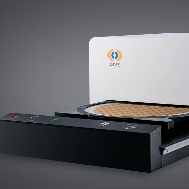
VEpioneer® is the world’s first fully integrated one-button bench-top Hyperspectral Vision system, tailored to your needs with the AI-equipped software VEsolve® Pro. Available in a standard and cleanroom version.
SYSTEM SOLUTIONS
VEpioneer + VEsolve® Pro
VEpioneer® is the world’s first fully integrated one-button bench-top Hyperspectral Vision system, tailored to your needs with the AI-equipped software VEsolve® Pro. Available in a standard and cleanroom version.

SYSTEM SOLUTIONS
VEpioneer® + VEsolve® Pro
VEpioneer® is the world’s first fully integrated one-button bench-top Hyperspectral Vision system, tailored to your needs with the AI-equipped software VEsolve® Pro. Available in a standard and cleanroom version.

SYSTEM SOLUTIONS
VEpioneer® + VEsolve® Pro
VEpioneer® is the world’s first fully integrated one-button bench-top Hyperspectral Vision system, tailored to your needs with the AI-equipped software VEsolve® Pro. Available in a standard and cleanroom version.

MODULE SOLUTIONS
VEreveal + VEsolve® Pro
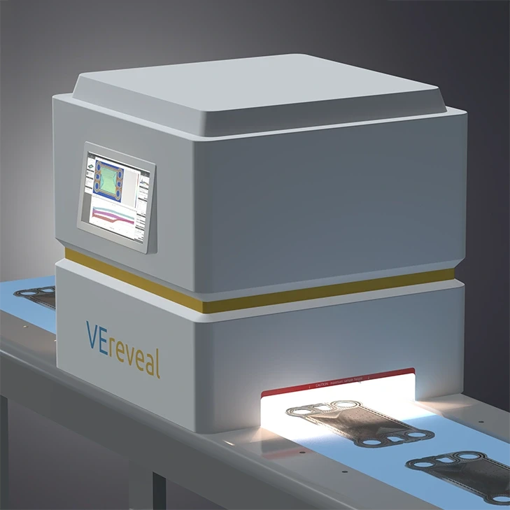
VEreveal features the VEpioneer® core for inline Hyperspectral Vision inspection, tailored to your needs with the AI-equipped software VEsolve® Pro.
MODULE SOLUTIONS
VEreveal + VEsolve® Pro
VEreveal features the VEpioneer® core for inline Hyperspectral Vision inspection, tailored to your needs with the AI-equipped software VEsolve® Pro.

MODULE SOLUTIONS
VEreveal + VEsolve® Pro
VEreveal features the VEpioneer® core for inline Hyperspectral Vision inspection, tailored to your needs with the AI-equipped software VEsolve® Pro.

MODULE SOLUTIONS
VEreveal + VEsolve® Pro
VEreveal features the VEpioneer® core for inline Hyperspectral Vision inspection, tailored to your needs with the AI-equipped software VEsolve® Pro.

Hyperspectral Vision comprehends the Invisible
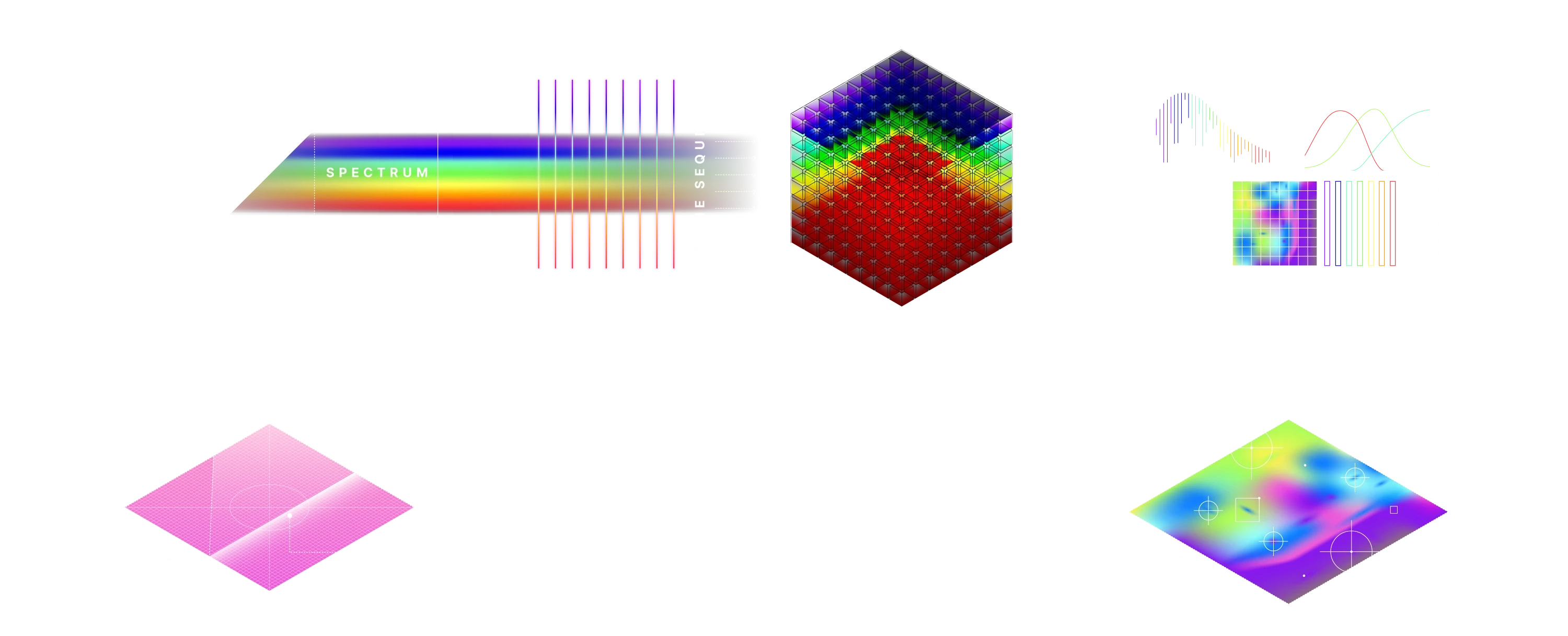
DIVE's hardware captures data in a data structure called ‚hypercube', enabling a fast and non-destructive inspection of the entire sample. The software then screens and explores the data using advanced machine learning algorithms, delivering actionable insights directly to the user.
DIVE's Hyperspectral Vision Applications
DIVE's Hyperspectral Vision Applications
DIVE's Hyperspectral Vision Applications
Bipolar Plates
Inspection of the anti-corrosion layer
on bipolar plates
Printed Circuit Boards (PCBs)
Inspection of PCB assembly quality
Wafer-based Products
Inspection of entire wafer surface
and layer thicknesses
Key Components in Fuel Cells and Electrolysers
DIVE's Hyperspectral Vision technology offers a fast, contactless, and comprehensive inspection of the anti-corrosion layer on bipolar plates. It provides spatially-resolved data on layer thickness, homogeneity, and defects across the entire bipolar plate.
Bipolar Plates
Inspection of the anti-corrosion layer
on bipolar plates
Printed Circuit Boards (PCBs)
Inspection of PCB assembly quality
Wafer-based Products
Inspection of entire wafer surface and layer thicknesses
Key Components in Fuel Cells and Electrolysers
DIVE's Hyperspectral Vision technology offers a fast, contactless, and comprehensive inspection of the anti-corrosion layer on bipolar plates. It provides spatially-resolved data on layer thickness, homogeneity, and defects across the entire bipolar plate.
Bipolar Plates
Inspection of the anti-corrosion layer
on bipolar plates
Printed Circuit Boards (PCBs)
Inspection of PCB assembly quality
Wafer-based Products
Inspection of entire wafer surface
and layer thicknesses
Key Components in Fuel Cells and Electrolysers
DIVE's Hyperspectral Vision technology offers a fast, contactless, and comprehensive inspection of the anti-corrosion layer on bipolar plates. It provides spatially-resolved data on layer thickness, homogeneity, and defects across the entire bipolar plate.
What our Clients and Partners have to say

Martin Landgraf
R & D Manager, Fraunhofer IPMS
“Hyperspectral imaging systems from DIVE provide the semiconductor industry with a new way of non-destructive testing of entire wafers. With support from Fraunhofer, DIVE is now making this innovative technology available for use in standard industrial cleanrooms, enabling significant productivity increases and cost reductions for semiconductor fabs.”
Frank Bösenberg
Managing Director, Silicon Saxony
“We're excited to have DIVE imaging systems as a member of Silicon Saxony. With their innovative technology, they are able to support the big semicon fabs in our network in their quest for a zero-defect production.”

Peter Friedrichs
Fellow SiC, Siltectra
“With the help of Hyperspectral Vision systems from DIVE, semiconductor manufacturing processes become comprehensible for the entire wafer surface. This matches perfectly to the high sophisticated wafer treatment processes at Siltectra.”
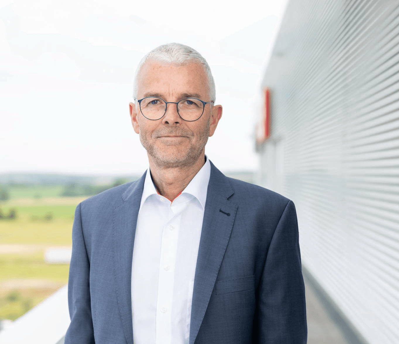
Dr. Dirk Drescher
Plant Manager, BOSCH Semiconductor Dresden
„The DIVE technology opens up a new dimension in surface metrology. It offers an innovative, expedited approach to uncovering and comprehending the intricate physics of thin film surfaces and interfaces.”

Peter Noelting
Senior Staff Engineer Tech Dev., Infineon Technologies Bipolar
„Together with DIVE, we are able to set up an incoming goods inspection that gives us direct information about further processing and necessary cleaning steps. In the future, we see an in-line application for Hyperspectral Vision as a target.“

Martin Landgraf
R & D Manager, Fraunhofer IPMS
“Hyperspectral imaging systems from DIVE provide the semiconductor industry with a new way of non-destructive testing of entire wafers. With support from Fraunhofer, DIVE is now making this innovative technology available for use in standard industrial cleanrooms, enabling significant productivity increases and cost reductions for semiconductor fabs.”

Frank Bösenberg
Managing Director, Silicon Saxony
“We're excited to have DIVE imaging systems as a member of Silicon Saxony. With their innovative technology, they are able to support the big semicon fabs in our network in their quest for a zero-defect production.”

Peter Friedrichs
Fellow SiC, Siltectra
“With the help of Hyperspectral Vision systems from DIVE, semiconductor manufacturing processes become comprehensible for the entire wafer surface. This matches perfectly to the high sophisticated wafer treatment processes at Siltectra.”

Dr. Dirk Drescher
Plant Manager, BOSCH Semiconductor Dresden
„The DIVE technology opens up a new dimension in surface metrology. It offers an innovative, expedited approach to uncovering and comprehending the intricate physics of thin film surfaces and interfaces.”

Peter Noelting
Senior Staff Engineer Tech Dev., Infineon Technologies Bipolar
„Together with DIVE, we are able to set up an incoming goods inspection that gives us direct information about further processing and necessary cleaning steps. In the future, we see an in-line application for Hyperspectral Vision as a target.“

Martin Landgraf
R & D Manager, Fraunhofer IPMS
“Hyperspectral imaging systems from DIVE provide the semiconductor industry with a new way of non-destructive testing of entire wafers. With support from Fraunhofer, DIVE is now making this innovative technology available for use in standard industrial cleanrooms, enabling significant productivity increases and cost reductions for semiconductor fabs.”

Frank Bösenberg
Managing Director, Silicon Saxony
“We're excited to have DIVE imaging systems as a member of Silicon Saxony. With their innovative technology, they are able to support the big semicon fabs in our network in their quest for a zero-defect production.”

Peter Friedrichs
Fellow SiC, Siltectra
“With the help of Hyperspectral Vision systems from DIVE, semiconductor manufacturing processes become comprehensible for the entire wafer surface. This matches perfectly to the high sophisticated wafer treatment processes at Siltectra.”

Dr. Dirk Drescher
Plant Manager, BOSCH Semiconductor Dresden
„The DIVE technology opens up a new dimension in surface metrology. It offers an innovative, expedited approach to uncovering and comprehending the intricate physics of thin film surfaces and interfaces.”

Peter Noelting
Senior Staff Engineer Tech Dev., Infineon Technologies Bipolar
„Together with DIVE, we are able to set up an incoming goods inspection that gives us direct information about further processing and necessary cleaning steps. In the future, we see an in-line application for Hyperspectral Vision as a target.“

Martin Landgraf
R & D Manager, Fraunhofer IPMS
“Hyperspectral imaging systems from DIVE provide the semiconductor industry with a new way of non-destructive testing of entire wafers. With support from Fraunhofer, DIVE is now making this innovative technology available for use in standard industrial cleanrooms, enabling significant productivity increases and cost reductions for semiconductor fabs.”

Frank Bösenberg
Managing Director, Silicon Saxony
“We're excited to have DIVE imaging systems as a member of Silicon Saxony. With their innovative technology, they are able to support the big semicon fabs in our network in their quest for a zero-defect production.”

Peter Friedrichs
Fellow SiC, Siltectra
“With the help of Hyperspectral Vision systems from DIVE, semiconductor manufacturing processes become comprehensible for the entire wafer surface. This matches perfectly to the high sophisticated wafer treatment processes at Siltectra.”

Dr. Dirk Drescher
Plant Manager, BOSCH Semiconductor Dresden
„The DIVE technology opens up a new dimension in surface metrology. It offers an innovative, expedited approach to uncovering and comprehending the intricate physics of thin film surfaces and interfaces.”

Peter Noelting
Senior Staff Engineer Tech Dev., Infineon Technologies Bipolar
„Together with DIVE, we are able to set up an incoming goods inspection that gives us direct information about further processing and necessary cleaning steps. In the future, we see an in-line application for Hyperspectral Vision as a target.“

Martin Landgraf
R & D Manager, Fraunhofer IPMS
“Hyperspectral imaging systems from DIVE provide the semiconductor industry with a new way of non-destructive testing of entire wafers. With support from Fraunhofer, DIVE is now making this innovative technology available for use in standard industrial cleanrooms, enabling significant productivity increases and cost reductions for semiconductor fabs.”

Frank Bösenberg
Managing Director, Silicon Saxony
“We're excited to have DIVE imaging systems as a member of Silicon Saxony. With their innovative technology, they are able to support the big semicon fabs in our network in their quest for a zero-defect production.”

Peter Friedrichs
Fellow SiC, Siltectra
“With the help of Hyperspectral Vision systems from DIVE, semiconductor manufacturing processes become comprehensible for the entire wafer surface. This matches perfectly to the high sophisticated wafer treatment processes at Siltectra.”

Dr. Dirk Drescher
Plant Manager, BOSCH Semiconductor Dresden
„The DIVE technology opens up a new dimension in surface metrology. It offers an innovative, expedited approach to uncovering and comprehending the intricate physics of thin film surfaces and interfaces.”

Peter Noelting
Senior Staff Engineer Tech Dev., Infineon Technologies Bipolar
„Together with DIVE, we are able to set up an incoming goods inspection that gives us direct information about further processing and necessary cleaning steps. In the future, we see an in-line application for Hyperspectral Vision as a target.“

Martin Landgraf
R & D Manager, Fraunhofer IPMS
“Hyperspectral imaging systems from DIVE provide the semiconductor industry with a new way of non-destructive testing of entire wafers. With support from Fraunhofer, DIVE is now making this innovative technology available for use in standard industrial cleanrooms, enabling significant productivity increases and cost reductions for semiconductor fabs.”

Frank Bösenberg
Managing Director, Silicon Saxony
“We're excited to have DIVE imaging systems as a member of Silicon Saxony. With their innovative technology, they are able to support the big semicon fabs in our network in their quest for a zero-defect production.”

Peter Friedrichs
Fellow SiC, Siltectra
“With the help of Hyperspectral Vision systems from DIVE, semiconductor manufacturing processes become comprehensible for the entire wafer surface. This matches perfectly to the high sophisticated wafer treatment processes at Siltectra.”

Dr. Dirk Drescher
Plant Manager, BOSCH Semiconductor Dresden
„The DIVE technology opens up a new dimension in surface metrology. It offers an innovative, expedited approach to uncovering and comprehending the intricate physics of thin film surfaces and interfaces.”

Peter Noelting
Senior Staff Engineer Tech Dev., Infineon Technologies Bipolar
„Together with DIVE, we are able to set up an incoming goods inspection that gives us direct information about further processing and necessary cleaning steps. In the future, we see an in-line application for Hyperspectral Vision as a target.“

Martin Landgraf
R & D Manager, Fraunhofer IPMS
“Hyperspectral imaging systems from DIVE provide the semiconductor industry with a new way of non-destructive testing of entire wafers. With support from Fraunhofer, DIVE is now making this innovative technology available for use in standard industrial cleanrooms, enabling significant productivity increases and cost reductions for semiconductor fabs.”

Frank Bösenberg
Managing Director, Silicon Saxony
“We're excited to have DIVE imaging systems as a member of Silicon Saxony. With their innovative technology, they are able to support the big semicon fabs in our network in their quest for a zero-defect production.”

Peter Friedrichs
Fellow SiC, Siltectra
“With the help of Hyperspectral Vision systems from DIVE, semiconductor manufacturing processes become comprehensible for the entire wafer surface. This matches perfectly to the high sophisticated wafer treatment processes at Siltectra.”

Dr. Dirk Drescher
Plant Manager, BOSCH Semiconductor Dresden
„The DIVE technology opens up a new dimension in surface metrology. It offers an innovative, expedited approach to uncovering and comprehending the intricate physics of thin film surfaces and interfaces.”

Peter Noelting
Senior Staff Engineer Tech Dev., Infineon Technologies Bipolar
„Together with DIVE, we are able to set up an incoming goods inspection that gives us direct information about further processing and necessary cleaning steps. In the future, we see an in-line application for Hyperspectral Vision as a target.“

Martin Landgraf
R & D Manager, Fraunhofer IPMS
“Hyperspectral imaging systems from DIVE provide the semiconductor industry with a new way of non-destructive testing of entire wafers. With support from Fraunhofer, DIVE is now making this innovative technology available for use in standard industrial cleanrooms, enabling significant productivity increases and cost reductions for semiconductor fabs.”

Frank Bösenberg
Managing Director, Silicon Saxony
“We're excited to have DIVE imaging systems as a member of Silicon Saxony. With their innovative technology, they are able to support the big semicon fabs in our network in their quest for a zero-defect production.”

Peter Friedrichs
Fellow SiC, Siltectra
“With the help of Hyperspectral Vision systems from DIVE, semiconductor manufacturing processes become comprehensible for the entire wafer surface. This matches perfectly to the high sophisticated wafer treatment processes at Siltectra.”

Dr. Dirk Drescher
Plant Manager, BOSCH Semiconductor Dresden
„The DIVE technology opens up a new dimension in surface metrology. It offers an innovative, expedited approach to uncovering and comprehending the intricate physics of thin film surfaces and interfaces.”

Peter Noelting
Senior Staff Engineer Tech Dev., Infineon Technologies Bipolar
„Together with DIVE, we are able to set up an incoming goods inspection that gives us direct information about further processing and necessary cleaning steps. In the future, we see an in-line application for Hyperspectral Vision as a target.“

Martin Landgraf
R & D Manager, Fraunhofer IPMS
“Hyperspectral imaging systems from DIVE provide the semiconductor industry with a new way of non-destructive testing of entire wafers. With support from Fraunhofer, DIVE is now making this innovative technology available for use in standard industrial cleanrooms, enabling significant productivity increases and cost reductions for semiconductor fabs.”

Frank Bösenberg
Managing Director, Silicon Saxony
“We're excited to have DIVE imaging systems as a member of Silicon Saxony. With their innovative technology, they are able to support the big semicon fabs in our network in their quest for a zero-defect production.”

Peter Friedrichs
Fellow SiC, Siltectra
“With the help of Hyperspectral Vision systems from DIVE, semiconductor manufacturing processes become comprehensible for the entire wafer surface. This matches perfectly to the high sophisticated wafer treatment processes at Siltectra.”

Dr. Dirk Drescher
Plant Manager, BOSCH Semiconductor Dresden
„The DIVE technology opens up a new dimension in surface metrology. It offers an innovative, expedited approach to uncovering and comprehending the intricate physics of thin film surfaces and interfaces.”

Peter Noelting
Senior Staff Engineer Tech Dev., Infineon Technologies Bipolar
„Together with DIVE, we are able to set up an incoming goods inspection that gives us direct information about further processing and necessary cleaning steps. In the future, we see an in-line application for Hyperspectral Vision as a target.“

Martin Landgraf
R & D Manager, Fraunhofer IPMS
“Hyperspectral imaging systems from DIVE provide the semiconductor industry with a new way of non-destructive testing of entire wafers. With support from Fraunhofer, DIVE is now making this innovative technology available for use in standard industrial cleanrooms, enabling significant productivity increases and cost reductions for semiconductor fabs.”

Frank Bösenberg
Managing Director, Silicon Saxony
“We're excited to have DIVE imaging systems as a member of Silicon Saxony. With their innovative technology, they are able to support the big semicon fabs in our network in their quest for a zero-defect production.”

Peter Friedrichs
Fellow SiC, Siltectra
“With the help of Hyperspectral Vision systems from DIVE, semiconductor manufacturing processes become comprehensible for the entire wafer surface. This matches perfectly to the high sophisticated wafer treatment processes at Siltectra.”

Dr. Dirk Drescher
Plant Manager, BOSCH Semiconductor Dresden
„The DIVE technology opens up a new dimension in surface metrology. It offers an innovative, expedited approach to uncovering and comprehending the intricate physics of thin film surfaces and interfaces.”

Peter Noelting
Senior Staff Engineer Tech Dev., Infineon Technologies Bipolar
„Together with DIVE, we are able to set up an incoming goods inspection that gives us direct information about further processing and necessary cleaning steps. In the future, we see an in-line application for Hyperspectral Vision as a target.“

Martin Landgraf
R & D Manager, Fraunhofer IPMS
“Hyperspectral imaging systems from DIVE provide the semiconductor industry with a new way of non-destructive testing of entire wafers. With support from Fraunhofer, DIVE is now making this innovative technology available for use in standard industrial cleanrooms, enabling significant productivity increases and cost reductions for semiconductor fabs.”

Frank Bösenberg
Managing Director, Silicon Saxony
“We're excited to have DIVE imaging systems as a member of Silicon Saxony. With their innovative technology, they are able to support the big semicon fabs in our network in their quest for a zero-defect production.”

Peter Friedrichs
Fellow SiC, Siltectra
“With the help of Hyperspectral Vision systems from DIVE, semiconductor manufacturing processes become comprehensible for the entire wafer surface. This matches perfectly to the high sophisticated wafer treatment processes at Siltectra.”

Dr. Dirk Drescher
Plant Manager, BOSCH Semiconductor Dresden
„The DIVE technology opens up a new dimension in surface metrology. It offers an innovative, expedited approach to uncovering and comprehending the intricate physics of thin film surfaces and interfaces.”

Peter Noelting
Senior Staff Engineer Tech Dev., Infineon Technologies Bipolar
„Together with DIVE, we are able to set up an incoming goods inspection that gives us direct information about further processing and necessary cleaning steps. In the future, we see an in-line application for Hyperspectral Vision as a target.“

Martin Landgraf
R & D Manager, Fraunhofer IPMS
“Hyperspectral imaging systems from DIVE provide the semiconductor industry with a new way of non-destructive testing of entire wafers. With support from Fraunhofer, DIVE is now making this innovative technology available for use in standard industrial cleanrooms, enabling significant productivity increases and cost reductions for semiconductor fabs.”

Frank Bösenberg
Managing Director, Silicon Saxony
“We're excited to have DIVE imaging systems as a member of Silicon Saxony. With their innovative technology, they are able to support the big semicon fabs in our network in their quest for a zero-defect production.”

Peter Friedrichs
Fellow SiC, Siltectra
“With the help of Hyperspectral Vision systems from DIVE, semiconductor manufacturing processes become comprehensible for the entire wafer surface. This matches perfectly to the high sophisticated wafer treatment processes at Siltectra.”

Dr. Dirk Drescher
Plant Manager, BOSCH Semiconductor Dresden
„The DIVE technology opens up a new dimension in surface metrology. It offers an innovative, expedited approach to uncovering and comprehending the intricate physics of thin film surfaces and interfaces.”

Peter Noelting
Senior Staff Engineer Tech Dev., Infineon Technologies Bipolar
„Together with DIVE, we are able to set up an incoming goods inspection that gives us direct information about further processing and necessary cleaning steps. In the future, we see an in-line application for Hyperspectral Vision as a target.“

Martin Landgraf
R & D Manager, Fraunhofer IPMS
“Hyperspectral imaging systems from DIVE provide the semiconductor industry with a new way of non-destructive testing of entire wafers. With support from Fraunhofer, DIVE is now making this innovative technology available for use in standard industrial cleanrooms, enabling significant productivity increases and cost reductions for semiconductor fabs.”

Frank Bösenberg
Managing Director, Silicon Saxony
“We're excited to have DIVE imaging systems as a member of Silicon Saxony. With their innovative technology, they are able to support the big semicon fabs in our network in their quest for a zero-defect production.”

Peter Friedrichs
Fellow SiC, Siltectra
“With the help of Hyperspectral Vision systems from DIVE, semiconductor manufacturing processes become comprehensible for the entire wafer surface. This matches perfectly to the high sophisticated wafer treatment processes at Siltectra.”

Dr. Dirk Drescher
Plant Manager, BOSCH Semiconductor Dresden
„The DIVE technology opens up a new dimension in surface metrology. It offers an innovative, expedited approach to uncovering and comprehending the intricate physics of thin film surfaces and interfaces.”

Peter Noelting
Senior Staff Engineer Tech Dev., Infineon Technologies Bipolar
„Together with DIVE, we are able to set up an incoming goods inspection that gives us direct information about further processing and necessary cleaning steps. In the future, we see an in-line application for Hyperspectral Vision as a target.“

Martin Landgraf
R & D Manager, Fraunhofer IPMS
“Hyperspectral imaging systems from DIVE provide the semiconductor industry with a new way of non-destructive testing of entire wafers. With support from Fraunhofer, DIVE is now making this innovative technology available for use in standard industrial cleanrooms, enabling significant productivity increases and cost reductions for semiconductor fabs.”

Frank Bösenberg
Managing Director, Silicon Saxony
“We're excited to have DIVE imaging systems as a member of Silicon Saxony. With their innovative technology, they are able to support the big semicon fabs in our network in their quest for a zero-defect production.”

Peter Friedrichs
Fellow SiC, Siltectra
“With the help of Hyperspectral Vision systems from DIVE, semiconductor manufacturing processes become comprehensible for the entire wafer surface. This matches perfectly to the high sophisticated wafer treatment processes at Siltectra.”

Dr. Dirk Drescher
Plant Manager, BOSCH Semiconductor Dresden
„The DIVE technology opens up a new dimension in surface metrology. It offers an innovative, expedited approach to uncovering and comprehending the intricate physics of thin film surfaces and interfaces.”

Peter Noelting
Senior Staff Engineer Tech Dev., Infineon Technologies Bipolar
„Together with DIVE, we are able to set up an incoming goods inspection that gives us direct information about further processing and necessary cleaning steps. In the future, we see an in-line application for Hyperspectral Vision as a target.“

Martin Landgraf
R & D Manager, Fraunhofer IPMS
“Hyperspectral imaging systems from DIVE provide the semiconductor industry with a new way of non-destructive testing of entire wafers. With support from Fraunhofer, DIVE is now making this innovative technology available for use in standard industrial cleanrooms, enabling significant productivity increases and cost reductions for semiconductor fabs.”

Frank Bösenberg
Managing Director, Silicon Saxony
“We're excited to have DIVE imaging systems as a member of Silicon Saxony. With their innovative technology, they are able to support the big semicon fabs in our network in their quest for a zero-defect production.”

Peter Friedrichs
Fellow SiC, Siltectra
“With the help of Hyperspectral Vision systems from DIVE, semiconductor manufacturing processes become comprehensible for the entire wafer surface. This matches perfectly to the high sophisticated wafer treatment processes at Siltectra.”

Dr. Dirk Drescher
Plant Manager, BOSCH Semiconductor Dresden
„The DIVE technology opens up a new dimension in surface metrology. It offers an innovative, expedited approach to uncovering and comprehending the intricate physics of thin film surfaces and interfaces.”

Peter Noelting
Senior Staff Engineer Tech Dev., Infineon Technologies Bipolar
„Together with DIVE, we are able to set up an incoming goods inspection that gives us direct information about further processing and necessary cleaning steps. In the future, we see an in-line application for Hyperspectral Vision as a target.“

Martin Landgraf
R & D Manager, Fraunhofer IPMS
“Hyperspectral imaging systems from DIVE provide the semiconductor industry with a new way of non-destructive testing of entire wafers. With support from Fraunhofer, DIVE is now making this innovative technology available for use in standard industrial cleanrooms, enabling significant productivity increases and cost reductions for semiconductor fabs.”

Frank Bösenberg
Managing Director, Silicon Saxony
“We're excited to have DIVE imaging systems as a member of Silicon Saxony. With their innovative technology, they are able to support the big semicon fabs in our network in their quest for a zero-defect production.”

Peter Friedrichs
Fellow SiC, Siltectra
“With the help of Hyperspectral Vision systems from DIVE, semiconductor manufacturing processes become comprehensible for the entire wafer surface. This matches perfectly to the high sophisticated wafer treatment processes at Siltectra.”

Dr. Dirk Drescher
Plant Manager, BOSCH Semiconductor Dresden
„The DIVE technology opens up a new dimension in surface metrology. It offers an innovative, expedited approach to uncovering and comprehending the intricate physics of thin film surfaces and interfaces.”

Peter Noelting
Senior Staff Engineer Tech Dev., Infineon Technologies Bipolar
„Together with DIVE, we are able to set up an incoming goods inspection that gives us direct information about further processing and necessary cleaning steps. In the future, we see an in-line application for Hyperspectral Vision as a target.“
News and Events
News and Events
News and Events
News and Events
Get in touch with Wulf
Let's find out together how DIVE's Hyperspectral Vision solutions can empower you.

Dr. Wulf Grählert
Sales
Email Address
Get in touch with Wulf
Let's find out together how DIVE's Hyperspectral Vision solutions can empower you.

Dr. Wulf Grählert
Sales
Email Address
Get in touch with Wulf
Let's find out together how DIVE's Hyperspectral Vision solutions can empower you.

Dr. Wulf Grählert
Sales
Email Address
Get in touch with Wulf
Let's find out together how DIVE's Hyperspectral Vision solutions can empower you.

Dr. Wulf Grählert
Sales
Email Address
We would like to thank our partners and funding bodies for their support. DIVE is funded by the Federal Ministry for Economic Affairs and Climate Protection and the European Social Fund as part of the EXIST research transfer program (funding reference: 03EUTSN217). DIVE is supported by the European Regional Development Fund and the Just Transition Fund.
We would like to thank our partners and funding bodies for their support. DIVE is funded by the Federal Ministry for Economic Affairs and Climate Protection and the European Social Fund as part of the EXIST research transfer program (funding reference: 03EUTSN217). DIVE is supported by the European Regional Development Fund and the Just Transition Fund.


