Applications
DIVE’s technology ensures quality, functionality, and cost-efficiency for thin layer and performance surface manufacturing.

Applications
DIVE’s technology ensures quality, functionality, and cost-efficiency for thin layer and performance surface manufacturing.

Applications
DIVE’s technology ensures quality, functionality, and cost-efficiency for thin layer and performance surface manufacturing.

Applications
DIVE’s technology ensures quality, functionality, and cost-efficiency for thin layer and performance surface manufacturing.
OUR CLIENTS & PARTNERS

OUR CLIENTS & PARTNERS

OUR CLIENTS & PARTNERS

OUR CLIENTS & PARTNERS

DIVE's Hyperspectral Vision Applications
Bipolar Plates
Printed Circuit Boards
Wafer-based Products
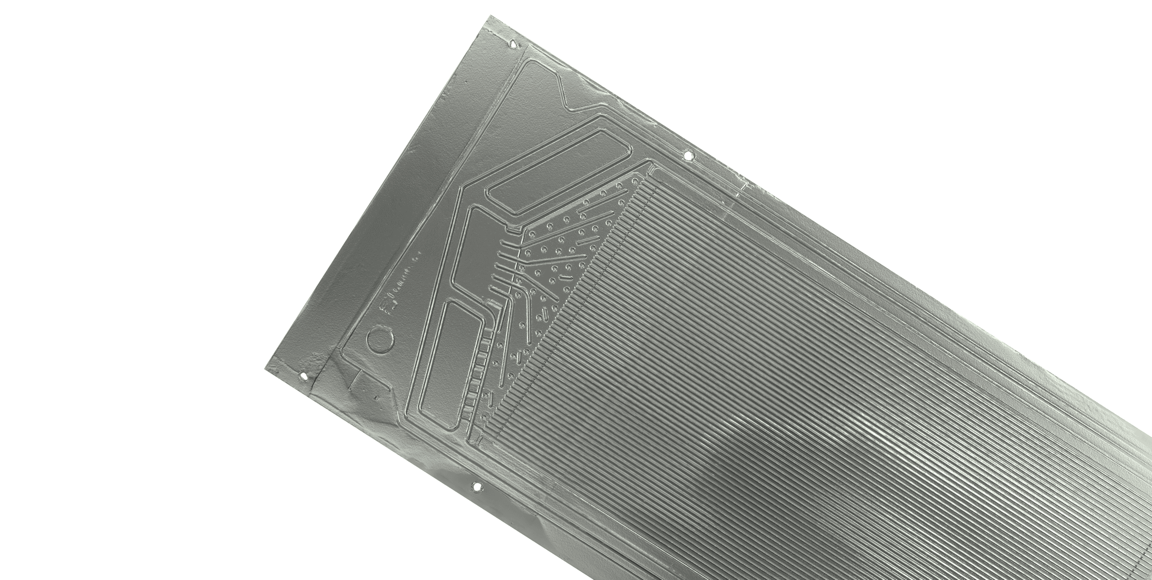
Bipolar plates are key components in fuel cells and electrolysers, acting as separators between individual cells. Corrosion protection of metallic bipolar plates is crucial, as the surrounding water gradually degrades the material, compromising performance and ultimately leading to the failure of the product. The inspection of these anti-corrosion layers faces limitations, particularly in production environments.
DIVE's Hyperspectral Vision technology offers a fast, contactless, and comprehensive inspection of the anti-corrosion layer on bipolar plates. It provides spatially-resolved data on layer thickness, homogeneity, and defects across the entire bipolar plate.

DIVE's Technology in manufacturing Processes

Layer deposition
(Large area) Manufacturing processes of thin films in industry require a precise control of e.g. film thickness, homogeneity, chemical compositions, crystallinity and surface roughness. In order to determine these properties in real time, Hyperspectral Vision is a novel, cost-efficient, and fast tool as in-line technology for large-area quality control. Manufacturing processes: - PVD - CVD - ALD - Spin coating - Slot-die coating - Spray coating

Layer and surface modification
Coating and surface modifications are of crucial importance in the industry as they add new functionalities to a surface in a very cost-efficient way. This must be accompanied by accurate monitoring of process parameters and modification results. Hyperspectral Vision provides insights into the surface condition (e.g. wettability, degree of adsorption, phase composition, penetration depth). Manufacturing processes: - Laser ablation -Laser microstructering - Doping - Etching - Thermal annealing

Surface cleaning
The cleanliness of surfaces has a major influence on the overall success of a manufacturing process and the reject rate. Only Hyperspectral Vision can provide comprehensive and non-destructive/non-contact knowledge of residues from manufacturing processes or after cleaning steps. Time-consuming single point measurements (e. g. XPS, AES) can be replaced and quality inspection is accelerated. Manufacturing processes: - Plasma cleaning - (Wet) Etching - Laser cleaning - Evaporation
Hyperspectral Vision Case Studies
Explore the diverse applications of Hyperspectral Vision in the semiconductor industry.
Hyperspectral Vision Case Studies
Explore the diverse applications of Hyperspectral Vision in the semiconductor industry.
Hyperspectral Vision Case Studies
Explore the diverse applications of Hyperspectral Vision in the semiconductor industry.
Hyperspectral Vision Case Studies
Explore the diverse applications of Hyperspectral Vision in the semiconductor industry.

Hyperspectral Vision comprehends the invisible
DIVE's solutions offer users valuable insights from thin layer and surface inspections, impacting the performance of these layers and surfaces. These insights form the foundation for ensuring quality, functionality and cost-efficiency in manufacturing processes, including layer deposition, layer and surface modification, and surface cleaning.
What Our Clients and Partner Have to Say

Martin Landgraf
R & D Manager, Fraunhofer IPMS
“Hyperspectral imaging systems from DIVE provide the semiconductor industry with a new way of non-destructive testing of entire wafers. With support from Fraunhofer, DIVE is now making this innovative technology available for use in standard industrial cleanrooms, enabling significant productivity increases and cost reductions for semiconductor fabs.”
Frank Bösenberg
Managing Director, Silicon Saxony
“We're excited to have DIVE imaging systems as a member of Silicon Saxony. With their innovative technology, they are able to support the big semicon fabs in our network in their quest for a zero-defect production.”

Peter Friedrichs
Fellow SiC, Siltectra
“With the help of Hyperspectral Vision systems from DIVE, semiconductor manufacturing processes become comprehensible for the entire wafer surface. This matches perfectly to the high sophisticated wafer treatment processes at Siltectra.”

Dr. Dirk Drescher
Plant Manager, BOSCH Semiconductor Dresden
„The DIVE technology opens up a new dimension in surface metrology. It offers an innovative, expedited approach to uncovering and comprehending the intricate physics of thin film surfaces and interfaces.”

Peter Noelting
Senior Staff Engineer Tech Dev., Infineon Technologies Bipolar
„Together with DIVE, we are able to set up an incoming goods inspection that gives us direct information about further processing and necessary cleaning steps. In the future, we see an in-line application for Hyperspectral Vision as a target.“

Martin Landgraf
R & D Manager, Fraunhofer IPMS
“Hyperspectral imaging systems from DIVE provide the semiconductor industry with a new way of non-destructive testing of entire wafers. With support from Fraunhofer, DIVE is now making this innovative technology available for use in standard industrial cleanrooms, enabling significant productivity increases and cost reductions for semiconductor fabs.”

Frank Bösenberg
Managing Director, Silicon Saxony
“We're excited to have DIVE imaging systems as a member of Silicon Saxony. With their innovative technology, they are able to support the big semicon fabs in our network in their quest for a zero-defect production.”

Peter Friedrichs
Fellow SiC, Siltectra
“With the help of Hyperspectral Vision systems from DIVE, semiconductor manufacturing processes become comprehensible for the entire wafer surface. This matches perfectly to the high sophisticated wafer treatment processes at Siltectra.”

Dr. Dirk Drescher
Plant Manager, BOSCH Semiconductor Dresden
„The DIVE technology opens up a new dimension in surface metrology. It offers an innovative, expedited approach to uncovering and comprehending the intricate physics of thin film surfaces and interfaces.”

Peter Noelting
Senior Staff Engineer Tech Dev., Infineon Technologies Bipolar
„Together with DIVE, we are able to set up an incoming goods inspection that gives us direct information about further processing and necessary cleaning steps. In the future, we see an in-line application for Hyperspectral Vision as a target.“

Martin Landgraf
R & D Manager, Fraunhofer IPMS
“Hyperspectral imaging systems from DIVE provide the semiconductor industry with a new way of non-destructive testing of entire wafers. With support from Fraunhofer, DIVE is now making this innovative technology available for use in standard industrial cleanrooms, enabling significant productivity increases and cost reductions for semiconductor fabs.”

Frank Bösenberg
Managing Director, Silicon Saxony
“We're excited to have DIVE imaging systems as a member of Silicon Saxony. With their innovative technology, they are able to support the big semicon fabs in our network in their quest for a zero-defect production.”

Peter Friedrichs
Fellow SiC, Siltectra
“With the help of Hyperspectral Vision systems from DIVE, semiconductor manufacturing processes become comprehensible for the entire wafer surface. This matches perfectly to the high sophisticated wafer treatment processes at Siltectra.”

Dr. Dirk Drescher
Plant Manager, BOSCH Semiconductor Dresden
„The DIVE technology opens up a new dimension in surface metrology. It offers an innovative, expedited approach to uncovering and comprehending the intricate physics of thin film surfaces and interfaces.”

Peter Noelting
Senior Staff Engineer Tech Dev., Infineon Technologies Bipolar
„Together with DIVE, we are able to set up an incoming goods inspection that gives us direct information about further processing and necessary cleaning steps. In the future, we see an in-line application for Hyperspectral Vision as a target.“

Martin Landgraf
R & D Manager, Fraunhofer IPMS
“Hyperspectral imaging systems from DIVE provide the semiconductor industry with a new way of non-destructive testing of entire wafers. With support from Fraunhofer, DIVE is now making this innovative technology available for use in standard industrial cleanrooms, enabling significant productivity increases and cost reductions for semiconductor fabs.”

Frank Bösenberg
Managing Director, Silicon Saxony
“We're excited to have DIVE imaging systems as a member of Silicon Saxony. With their innovative technology, they are able to support the big semicon fabs in our network in their quest for a zero-defect production.”

Peter Friedrichs
Fellow SiC, Siltectra
“With the help of Hyperspectral Vision systems from DIVE, semiconductor manufacturing processes become comprehensible for the entire wafer surface. This matches perfectly to the high sophisticated wafer treatment processes at Siltectra.”

Dr. Dirk Drescher
Plant Manager, BOSCH Semiconductor Dresden
„The DIVE technology opens up a new dimension in surface metrology. It offers an innovative, expedited approach to uncovering and comprehending the intricate physics of thin film surfaces and interfaces.”

Peter Noelting
Senior Staff Engineer Tech Dev., Infineon Technologies Bipolar
„Together with DIVE, we are able to set up an incoming goods inspection that gives us direct information about further processing and necessary cleaning steps. In the future, we see an in-line application for Hyperspectral Vision as a target.“

Martin Landgraf
R & D Manager, Fraunhofer IPMS
“Hyperspectral imaging systems from DIVE provide the semiconductor industry with a new way of non-destructive testing of entire wafers. With support from Fraunhofer, DIVE is now making this innovative technology available for use in standard industrial cleanrooms, enabling significant productivity increases and cost reductions for semiconductor fabs.”

Frank Bösenberg
Managing Director, Silicon Saxony
“We're excited to have DIVE imaging systems as a member of Silicon Saxony. With their innovative technology, they are able to support the big semicon fabs in our network in their quest for a zero-defect production.”

Peter Friedrichs
Fellow SiC, Siltectra
“With the help of Hyperspectral Vision systems from DIVE, semiconductor manufacturing processes become comprehensible for the entire wafer surface. This matches perfectly to the high sophisticated wafer treatment processes at Siltectra.”

Dr. Dirk Drescher
Plant Manager, BOSCH Semiconductor Dresden
„The DIVE technology opens up a new dimension in surface metrology. It offers an innovative, expedited approach to uncovering and comprehending the intricate physics of thin film surfaces and interfaces.”

Peter Noelting
Senior Staff Engineer Tech Dev., Infineon Technologies Bipolar
„Together with DIVE, we are able to set up an incoming goods inspection that gives us direct information about further processing and necessary cleaning steps. In the future, we see an in-line application for Hyperspectral Vision as a target.“

Martin Landgraf
R & D Manager, Fraunhofer IPMS
“Hyperspectral imaging systems from DIVE provide the semiconductor industry with a new way of non-destructive testing of entire wafers. With support from Fraunhofer, DIVE is now making this innovative technology available for use in standard industrial cleanrooms, enabling significant productivity increases and cost reductions for semiconductor fabs.”

Frank Bösenberg
Managing Director, Silicon Saxony
“We're excited to have DIVE imaging systems as a member of Silicon Saxony. With their innovative technology, they are able to support the big semicon fabs in our network in their quest for a zero-defect production.”

Peter Friedrichs
Fellow SiC, Siltectra
“With the help of Hyperspectral Vision systems from DIVE, semiconductor manufacturing processes become comprehensible for the entire wafer surface. This matches perfectly to the high sophisticated wafer treatment processes at Siltectra.”

Dr. Dirk Drescher
Plant Manager, BOSCH Semiconductor Dresden
„The DIVE technology opens up a new dimension in surface metrology. It offers an innovative, expedited approach to uncovering and comprehending the intricate physics of thin film surfaces and interfaces.”

Peter Noelting
Senior Staff Engineer Tech Dev., Infineon Technologies Bipolar
„Together with DIVE, we are able to set up an incoming goods inspection that gives us direct information about further processing and necessary cleaning steps. In the future, we see an in-line application for Hyperspectral Vision as a target.“

Martin Landgraf
R & D Manager, Fraunhofer IPMS
“Hyperspectral imaging systems from DIVE provide the semiconductor industry with a new way of non-destructive testing of entire wafers. With support from Fraunhofer, DIVE is now making this innovative technology available for use in standard industrial cleanrooms, enabling significant productivity increases and cost reductions for semiconductor fabs.”

Frank Bösenberg
Managing Director, Silicon Saxony
“We're excited to have DIVE imaging systems as a member of Silicon Saxony. With their innovative technology, they are able to support the big semicon fabs in our network in their quest for a zero-defect production.”

Peter Friedrichs
Fellow SiC, Siltectra
“With the help of Hyperspectral Vision systems from DIVE, semiconductor manufacturing processes become comprehensible for the entire wafer surface. This matches perfectly to the high sophisticated wafer treatment processes at Siltectra.”

Dr. Dirk Drescher
Plant Manager, BOSCH Semiconductor Dresden
„The DIVE technology opens up a new dimension in surface metrology. It offers an innovative, expedited approach to uncovering and comprehending the intricate physics of thin film surfaces and interfaces.”

Peter Noelting
Senior Staff Engineer Tech Dev., Infineon Technologies Bipolar
„Together with DIVE, we are able to set up an incoming goods inspection that gives us direct information about further processing and necessary cleaning steps. In the future, we see an in-line application for Hyperspectral Vision as a target.“

Martin Landgraf
R & D Manager, Fraunhofer IPMS
“Hyperspectral imaging systems from DIVE provide the semiconductor industry with a new way of non-destructive testing of entire wafers. With support from Fraunhofer, DIVE is now making this innovative technology available for use in standard industrial cleanrooms, enabling significant productivity increases and cost reductions for semiconductor fabs.”

Frank Bösenberg
Managing Director, Silicon Saxony
“We're excited to have DIVE imaging systems as a member of Silicon Saxony. With their innovative technology, they are able to support the big semicon fabs in our network in their quest for a zero-defect production.”

Peter Friedrichs
Fellow SiC, Siltectra
“With the help of Hyperspectral Vision systems from DIVE, semiconductor manufacturing processes become comprehensible for the entire wafer surface. This matches perfectly to the high sophisticated wafer treatment processes at Siltectra.”

Dr. Dirk Drescher
Plant Manager, BOSCH Semiconductor Dresden
„The DIVE technology opens up a new dimension in surface metrology. It offers an innovative, expedited approach to uncovering and comprehending the intricate physics of thin film surfaces and interfaces.”

Peter Noelting
Senior Staff Engineer Tech Dev., Infineon Technologies Bipolar
„Together with DIVE, we are able to set up an incoming goods inspection that gives us direct information about further processing and necessary cleaning steps. In the future, we see an in-line application for Hyperspectral Vision as a target.“

Martin Landgraf
R & D Manager, Fraunhofer IPMS
“Hyperspectral imaging systems from DIVE provide the semiconductor industry with a new way of non-destructive testing of entire wafers. With support from Fraunhofer, DIVE is now making this innovative technology available for use in standard industrial cleanrooms, enabling significant productivity increases and cost reductions for semiconductor fabs.”

Frank Bösenberg
Managing Director, Silicon Saxony
“We're excited to have DIVE imaging systems as a member of Silicon Saxony. With their innovative technology, they are able to support the big semicon fabs in our network in their quest for a zero-defect production.”

Peter Friedrichs
Fellow SiC, Siltectra
“With the help of Hyperspectral Vision systems from DIVE, semiconductor manufacturing processes become comprehensible for the entire wafer surface. This matches perfectly to the high sophisticated wafer treatment processes at Siltectra.”

Dr. Dirk Drescher
Plant Manager, BOSCH Semiconductor Dresden
„The DIVE technology opens up a new dimension in surface metrology. It offers an innovative, expedited approach to uncovering and comprehending the intricate physics of thin film surfaces and interfaces.”

Peter Noelting
Senior Staff Engineer Tech Dev., Infineon Technologies Bipolar
„Together with DIVE, we are able to set up an incoming goods inspection that gives us direct information about further processing and necessary cleaning steps. In the future, we see an in-line application for Hyperspectral Vision as a target.“

Martin Landgraf
R & D Manager, Fraunhofer IPMS
“Hyperspectral imaging systems from DIVE provide the semiconductor industry with a new way of non-destructive testing of entire wafers. With support from Fraunhofer, DIVE is now making this innovative technology available for use in standard industrial cleanrooms, enabling significant productivity increases and cost reductions for semiconductor fabs.”

Frank Bösenberg
Managing Director, Silicon Saxony
“We're excited to have DIVE imaging systems as a member of Silicon Saxony. With their innovative technology, they are able to support the big semicon fabs in our network in their quest for a zero-defect production.”

Peter Friedrichs
Fellow SiC, Siltectra
“With the help of Hyperspectral Vision systems from DIVE, semiconductor manufacturing processes become comprehensible for the entire wafer surface. This matches perfectly to the high sophisticated wafer treatment processes at Siltectra.”

Dr. Dirk Drescher
Plant Manager, BOSCH Semiconductor Dresden
„The DIVE technology opens up a new dimension in surface metrology. It offers an innovative, expedited approach to uncovering and comprehending the intricate physics of thin film surfaces and interfaces.”

Peter Noelting
Senior Staff Engineer Tech Dev., Infineon Technologies Bipolar
„Together with DIVE, we are able to set up an incoming goods inspection that gives us direct information about further processing and necessary cleaning steps. In the future, we see an in-line application for Hyperspectral Vision as a target.“

Martin Landgraf
R & D Manager, Fraunhofer IPMS
“Hyperspectral imaging systems from DIVE provide the semiconductor industry with a new way of non-destructive testing of entire wafers. With support from Fraunhofer, DIVE is now making this innovative technology available for use in standard industrial cleanrooms, enabling significant productivity increases and cost reductions for semiconductor fabs.”

Frank Bösenberg
Managing Director, Silicon Saxony
“We're excited to have DIVE imaging systems as a member of Silicon Saxony. With their innovative technology, they are able to support the big semicon fabs in our network in their quest for a zero-defect production.”

Peter Friedrichs
Fellow SiC, Siltectra
“With the help of Hyperspectral Vision systems from DIVE, semiconductor manufacturing processes become comprehensible for the entire wafer surface. This matches perfectly to the high sophisticated wafer treatment processes at Siltectra.”

Dr. Dirk Drescher
Plant Manager, BOSCH Semiconductor Dresden
„The DIVE technology opens up a new dimension in surface metrology. It offers an innovative, expedited approach to uncovering and comprehending the intricate physics of thin film surfaces and interfaces.”

Peter Noelting
Senior Staff Engineer Tech Dev., Infineon Technologies Bipolar
„Together with DIVE, we are able to set up an incoming goods inspection that gives us direct information about further processing and necessary cleaning steps. In the future, we see an in-line application for Hyperspectral Vision as a target.“

Martin Landgraf
R & D Manager, Fraunhofer IPMS
“Hyperspectral imaging systems from DIVE provide the semiconductor industry with a new way of non-destructive testing of entire wafers. With support from Fraunhofer, DIVE is now making this innovative technology available for use in standard industrial cleanrooms, enabling significant productivity increases and cost reductions for semiconductor fabs.”

Frank Bösenberg
Managing Director, Silicon Saxony
“We're excited to have DIVE imaging systems as a member of Silicon Saxony. With their innovative technology, they are able to support the big semicon fabs in our network in their quest for a zero-defect production.”

Peter Friedrichs
Fellow SiC, Siltectra
“With the help of Hyperspectral Vision systems from DIVE, semiconductor manufacturing processes become comprehensible for the entire wafer surface. This matches perfectly to the high sophisticated wafer treatment processes at Siltectra.”

Dr. Dirk Drescher
Plant Manager, BOSCH Semiconductor Dresden
„The DIVE technology opens up a new dimension in surface metrology. It offers an innovative, expedited approach to uncovering and comprehending the intricate physics of thin film surfaces and interfaces.”

Peter Noelting
Senior Staff Engineer Tech Dev., Infineon Technologies Bipolar
„Together with DIVE, we are able to set up an incoming goods inspection that gives us direct information about further processing and necessary cleaning steps. In the future, we see an in-line application for Hyperspectral Vision as a target.“

Martin Landgraf
R & D Manager, Fraunhofer IPMS
“Hyperspectral imaging systems from DIVE provide the semiconductor industry with a new way of non-destructive testing of entire wafers. With support from Fraunhofer, DIVE is now making this innovative technology available for use in standard industrial cleanrooms, enabling significant productivity increases and cost reductions for semiconductor fabs.”

Frank Bösenberg
Managing Director, Silicon Saxony
“We're excited to have DIVE imaging systems as a member of Silicon Saxony. With their innovative technology, they are able to support the big semicon fabs in our network in their quest for a zero-defect production.”

Peter Friedrichs
Fellow SiC, Siltectra
“With the help of Hyperspectral Vision systems from DIVE, semiconductor manufacturing processes become comprehensible for the entire wafer surface. This matches perfectly to the high sophisticated wafer treatment processes at Siltectra.”

Dr. Dirk Drescher
Plant Manager, BOSCH Semiconductor Dresden
„The DIVE technology opens up a new dimension in surface metrology. It offers an innovative, expedited approach to uncovering and comprehending the intricate physics of thin film surfaces and interfaces.”

Peter Noelting
Senior Staff Engineer Tech Dev., Infineon Technologies Bipolar
„Together with DIVE, we are able to set up an incoming goods inspection that gives us direct information about further processing and necessary cleaning steps. In the future, we see an in-line application for Hyperspectral Vision as a target.“

Martin Landgraf
R & D Manager, Fraunhofer IPMS
“Hyperspectral imaging systems from DIVE provide the semiconductor industry with a new way of non-destructive testing of entire wafers. With support from Fraunhofer, DIVE is now making this innovative technology available for use in standard industrial cleanrooms, enabling significant productivity increases and cost reductions for semiconductor fabs.”

Frank Bösenberg
Managing Director, Silicon Saxony
“We're excited to have DIVE imaging systems as a member of Silicon Saxony. With their innovative technology, they are able to support the big semicon fabs in our network in their quest for a zero-defect production.”

Peter Friedrichs
Fellow SiC, Siltectra
“With the help of Hyperspectral Vision systems from DIVE, semiconductor manufacturing processes become comprehensible for the entire wafer surface. This matches perfectly to the high sophisticated wafer treatment processes at Siltectra.”

Dr. Dirk Drescher
Plant Manager, BOSCH Semiconductor Dresden
„The DIVE technology opens up a new dimension in surface metrology. It offers an innovative, expedited approach to uncovering and comprehending the intricate physics of thin film surfaces and interfaces.”

Peter Noelting
Senior Staff Engineer Tech Dev., Infineon Technologies Bipolar
„Together with DIVE, we are able to set up an incoming goods inspection that gives us direct information about further processing and necessary cleaning steps. In the future, we see an in-line application for Hyperspectral Vision as a target.“

Martin Landgraf
R & D Manager, Fraunhofer IPMS
“Hyperspectral imaging systems from DIVE provide the semiconductor industry with a new way of non-destructive testing of entire wafers. With support from Fraunhofer, DIVE is now making this innovative technology available for use in standard industrial cleanrooms, enabling significant productivity increases and cost reductions for semiconductor fabs.”

Frank Bösenberg
Managing Director, Silicon Saxony
“We're excited to have DIVE imaging systems as a member of Silicon Saxony. With their innovative technology, they are able to support the big semicon fabs in our network in their quest for a zero-defect production.”

Peter Friedrichs
Fellow SiC, Siltectra
“With the help of Hyperspectral Vision systems from DIVE, semiconductor manufacturing processes become comprehensible for the entire wafer surface. This matches perfectly to the high sophisticated wafer treatment processes at Siltectra.”

Dr. Dirk Drescher
Plant Manager, BOSCH Semiconductor Dresden
„The DIVE technology opens up a new dimension in surface metrology. It offers an innovative, expedited approach to uncovering and comprehending the intricate physics of thin film surfaces and interfaces.”

Peter Noelting
Senior Staff Engineer Tech Dev., Infineon Technologies Bipolar
„Together with DIVE, we are able to set up an incoming goods inspection that gives us direct information about further processing and necessary cleaning steps. In the future, we see an in-line application for Hyperspectral Vision as a target.“

Martin Landgraf
R & D Manager, Fraunhofer IPMS
“Hyperspectral imaging systems from DIVE provide the semiconductor industry with a new way of non-destructive testing of entire wafers. With support from Fraunhofer, DIVE is now making this innovative technology available for use in standard industrial cleanrooms, enabling significant productivity increases and cost reductions for semiconductor fabs.”

Frank Bösenberg
Managing Director, Silicon Saxony
“We're excited to have DIVE imaging systems as a member of Silicon Saxony. With their innovative technology, they are able to support the big semicon fabs in our network in their quest for a zero-defect production.”

Peter Friedrichs
Fellow SiC, Siltectra
“With the help of Hyperspectral Vision systems from DIVE, semiconductor manufacturing processes become comprehensible for the entire wafer surface. This matches perfectly to the high sophisticated wafer treatment processes at Siltectra.”

Dr. Dirk Drescher
Plant Manager, BOSCH Semiconductor Dresden
„The DIVE technology opens up a new dimension in surface metrology. It offers an innovative, expedited approach to uncovering and comprehending the intricate physics of thin film surfaces and interfaces.”

Peter Noelting
Senior Staff Engineer Tech Dev., Infineon Technologies Bipolar
„Together with DIVE, we are able to set up an incoming goods inspection that gives us direct information about further processing and necessary cleaning steps. In the future, we see an in-line application for Hyperspectral Vision as a target.“
Get in touch with Wulf
Let's find out together how DIVE's Hyperspectral Vision solutions can empower you.

Dr. Wulf Grählert
Sales
Email Address
Get in touch with Wulf
Let's find out together how DIVE's Hyperspectral Vision solutions can empower you.

Dr. Wulf Grählert
Sales
Email Address
Get in touch with Wulf
Let's find out together how DIVE's Hyperspectral Vision solutions can empower you.

Dr. Wulf Grählert
Sales
Email Address
Get in touch with Wulf
Let's find out together how DIVE's Hyperspectral Vision solutions can empower you.

Dr. Wulf Grählert
Sales
Email Address
We would like to thank our partners and funding bodies for their support. DIVE is funded by the Federal Ministry for Economic Affairs and Climate Protection and the European Social Fund as part of the EXIST research transfer program (funding reference: 03EUTSN217). DIVE is supported by the European Regional Development Fund and the Just Transition Fund.

