Oct 1, 2024
Power Electronics Cleanliness
Quantifying cleanliness of a direct bonded copper substrate after soldering across the entire substrate

Dr. Wulf Grählert
Sales & Customer Care
Power electronics substrates offer significant advantages over traditional printed circuit boards (PCBs) in high-voltage and high-current applications. Various interconnection techniques are employed in power electronics packaging, with soldering being the most prevalent. However, the soldering process introduces organic contaminants and residues, primarily stemming from the fluxes in solder pastes. They necessitate post-soldering cleaning to mitigate electrochemical migration, oxidation, corrosion, and subsequent adhesion degradation, ultimately preventing substrate failure.
The trend towards miniaturisation and increased power density in electronics manufacturing requires stringent cleanliness standards for power electronics substrates. While visual inspection remains a common practice in series production, it lacks an objective cleanliness assessment. Organic contamination levels, specifically surface carbon concentration, are critical indicators of substrate cleanliness. Several surface analysis techniques, including X-ray photoelectron spectroscopy (XPS), Auger electron spectroscopy (AES), and time-of-flight secondary ion mass spectrometry (TOF-SIMS), can quantify these contaminants. While capable all techniques are impractical for fast, comprehensive, and non-destructive inspection.
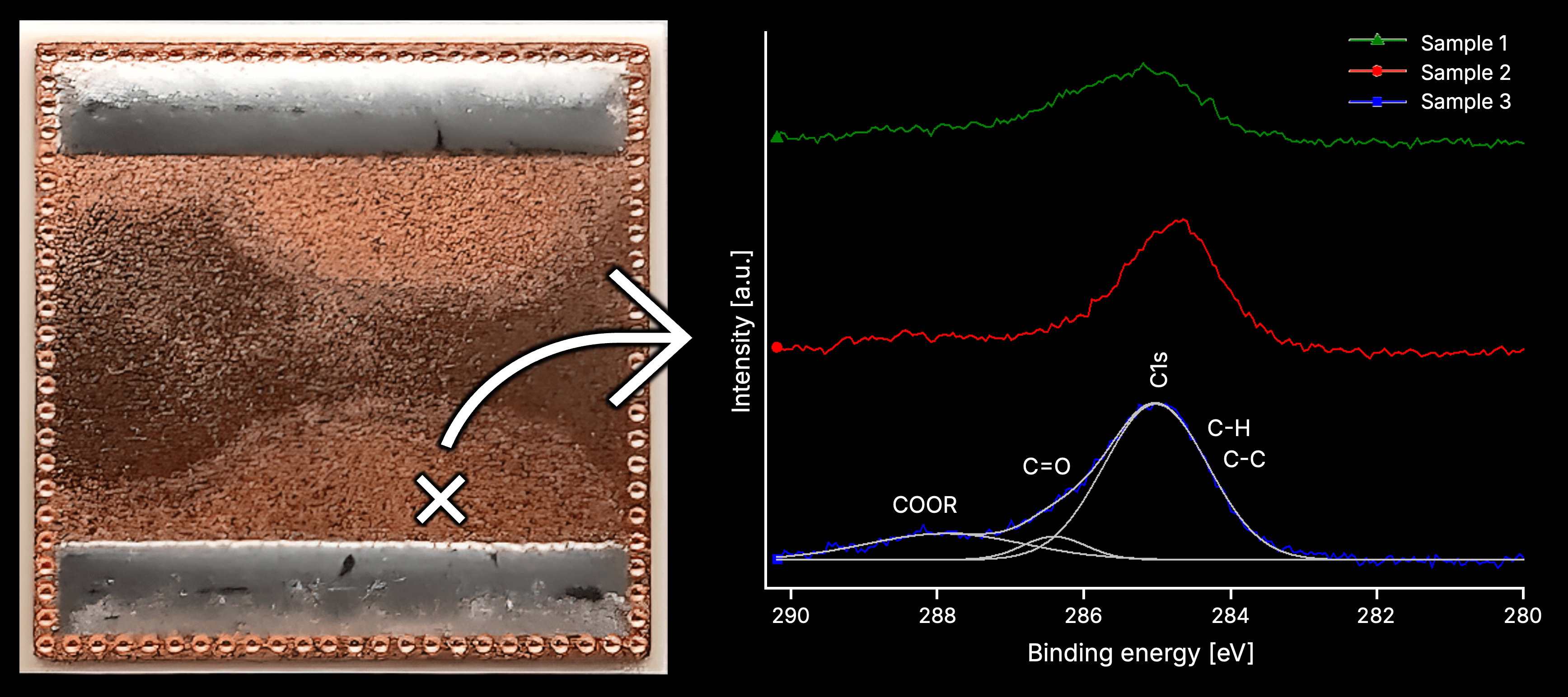
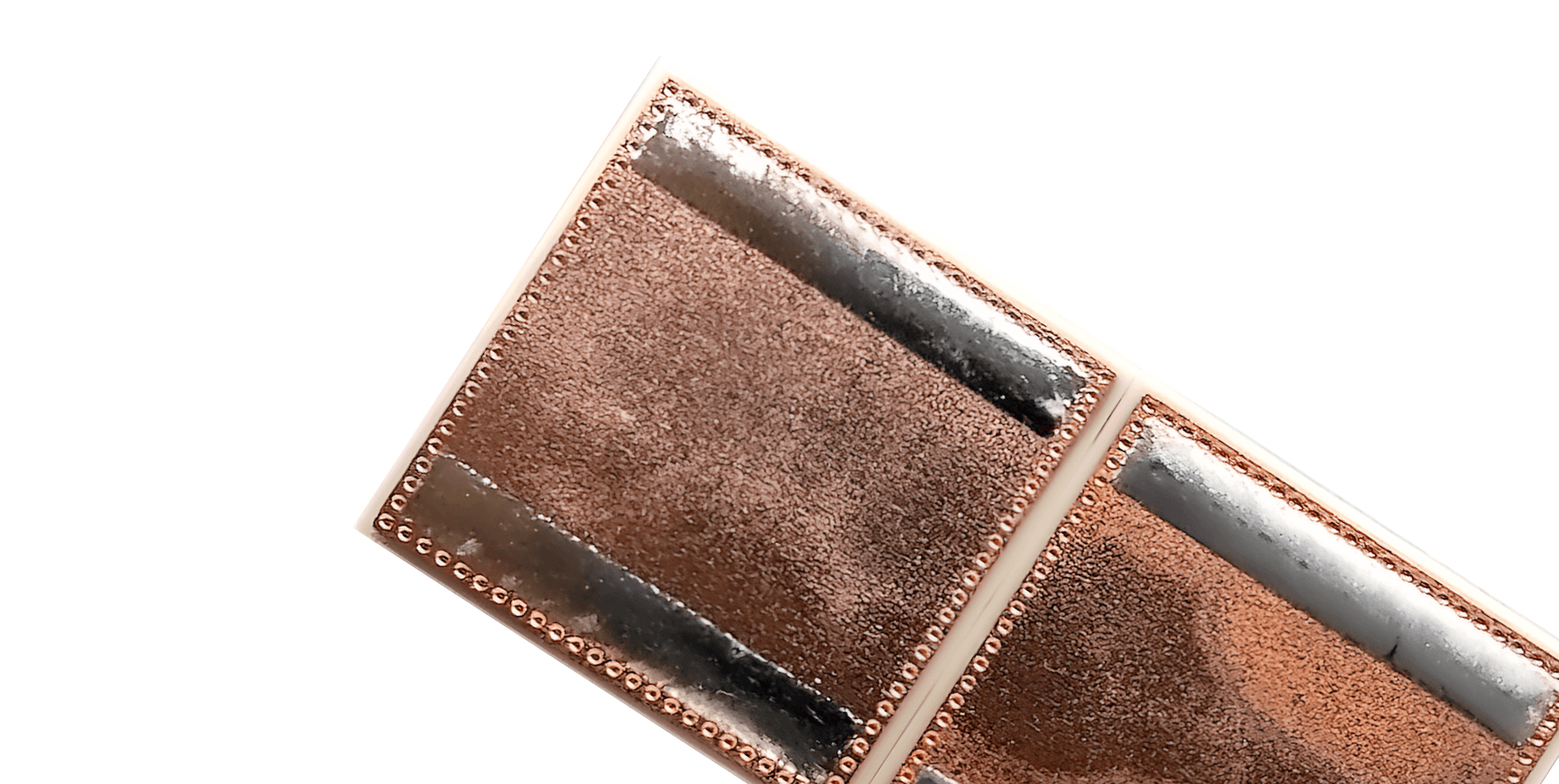
This case study examines a direct bonded copper (DBC) substrate (21 x 21 x 1.1 mm) with two 18 x 3 x 0.2 mm strips of F360 SnAg 3.5 solder paste. Following a cleaning process, XPS analysis was conducted at a specific point on the substrate (see image below). The resulting carbon spectra illustrate the influence of varying cleaning parameters on localized carbon concentration. While the measured carbon content 1 mm from the solder paste exhibits a range of 52 to 76 atom percent (At.-%), this localised measurement, encompassing an area of 100 µm x 100 µm, may not accurately represent the overall substrate cleanliness.

DIVE’s solution
Our at-line VEpioneer and in-line VEreveal systems allow to determine the surface cleanliness of a substrate after soldering with pixel-level precision. The entire substrate is analysed non-invasively in less than 6 seconds, with a spatial resolution of 150µm x 150µm per pixel.
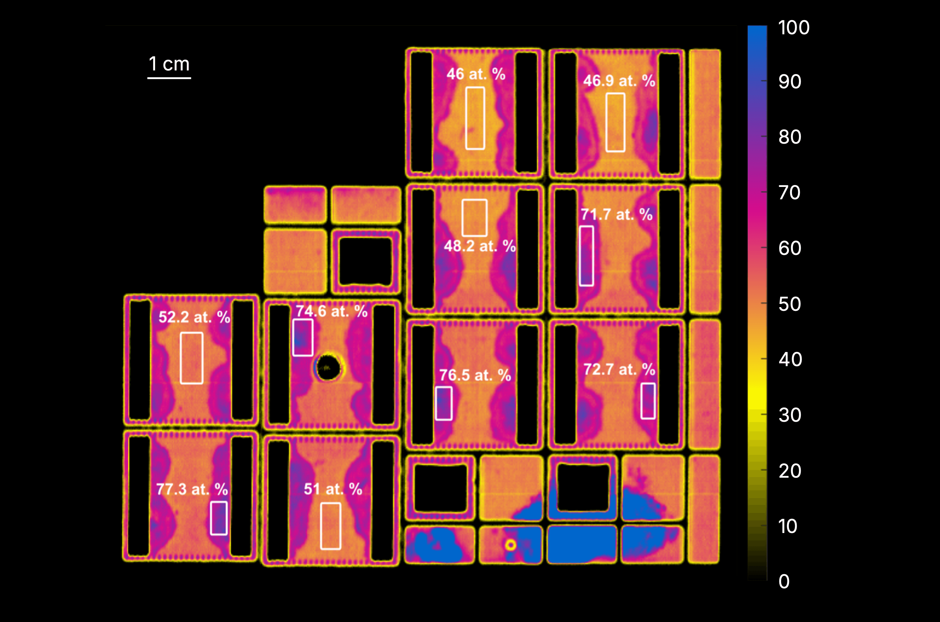
The image below presents a sample set of analysed substrates, where colour mapping visualizes the atomic percent of carbon content on the copper surface. This visualization demonstrates the non-homogeneous distribution of residual carbon contamination after cleaning. Mean carbon content values for selected areas (highlighted in white) are also displayed. The analysis achieves a root mean square error of 7.65 At.-%, with the potential for further improvement through expanded sample size.

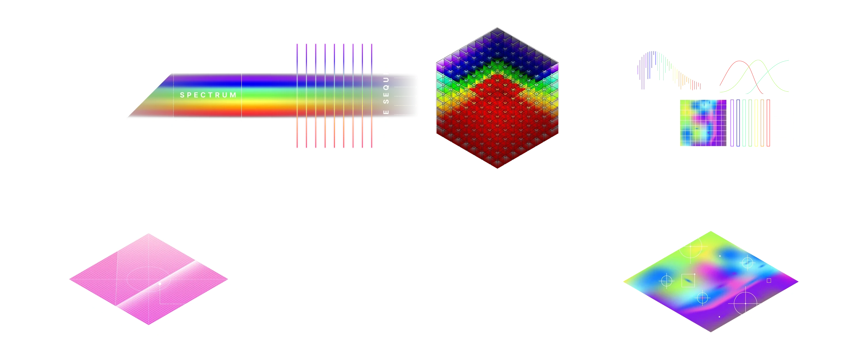
VEpioneer and VEreveal are built upon identical technological foundations and utilize our proprietary software suite, VEsolve Pro. The image below illustrates the operational workflow. Initially, data acquisition is performed via line-scan hyperspectral imaging, wherein the intensity of light reflected by the excited sample is measured. Spectral decomposition occurs within the camera, recording the intensity per pixel. Subsequent frame acquisition through sample translation results in the formation of the hyperspectral data cube. In the second phase, this data undergoes screening, exploration and analysis within VEsolve Pro, applying diverse machine learning algorithms. Finally, contingent on the selected algorithms, a wide spectrum of insights can be generated, encompassing layer thicknesses, electrical and mechanical surface properties, as well as the identification of defects and contaminants.

How the solution benefits our customers
Enhanced Reliability & Quality: Objective, comprehensive cleanliness analysis enables optimisation of the cleaning process and improves reliability of power electronics
Reduced Personnel Costs: Automated inspection eliminates labor costs associated with visual inspection by a trained operator
Advanced Miniaturisation: Precise cleanliness control facilitates further miniaturisation of power electronics and increased power density
Product portfolio
VEpioneer and VEreveal systems provide spatially resolved property images of surfaces and thin films. Properties may include layer thickness, surface roughness, defects and contaminations, chemical, electrical and optical properties or any other type of quality criteria. The systems can be tailored to specific applications through customizable options for sample stage, excitation source, spectral ranges, cleanroom compatibility, and software interfaces.
Partnering with you
The DIVE imaging systems GmbH is a German manufacturer of innovative spectral imaging solutions. Our VEpioneer system is the world’s first fully integrated, one-button bench-top Hyperspectral Vision system, combining high-performance imaging with advanced data analysis to deliver insights within milliseconds. DIVE products deliver at-line and in-line inspection with highest precision and ultra-fast measuring speeds from nano- to micrometers.
We would like to thank our partners and funding bodies for their support. DIVE is funded by the Federal Ministry for Economic Affairs and Climate Protection and the European Social Fund as part of the EXIST research transfer program (funding reference: 03EUTSN217). DIVE is supported by the European Regional Development Fund and the Just Transition Fund.


