Oct 17, 2024
Inspection of resist layer thickness on a wafer
Inspecting resist layer thickness after spin-coating across the entire wafer surface within 10 seconds with 300 µm x 300 µm spatial resolution to subsitute off-line inspection

Dr. Wulf Grählert
Sales and Customer Care
Photolithography is a crucial process in semiconductor manufacturing, employing light to define the patterns on wafers. These patterns serve as the foundation for the nanoscale circuits essential for logic and memory functions. The process involves the selective dissolution of a light-sensitive resist, according to the patterns present on lithographic masks. The resist is typically applied through a spin-coating process which involves rapidly rotating the wafer to distribute the deposited resist.
Precise control of resist thickness and homogeneity is critical in spin-coating processes. Uniformity ensures fidelity in subsequent time-controlled etching steps, where deviations can lead to incomplete resist removal or unintended substrate etching. While various metrology techniques like ellipsometry and Fourier-transform infrared spectroscopy (FT-IR) can accurately measure resist thickness, their implementation for fast and comprehensive in-line inspection presents practical challenges.
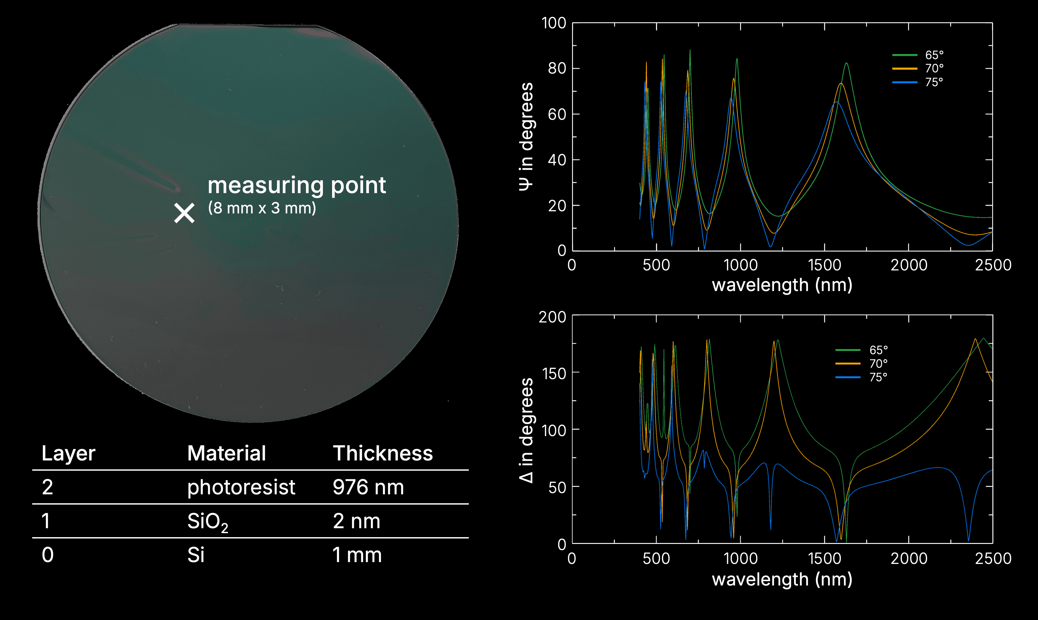
This case study analyses a 4-inch silicon wafer coated with a resist layer following a soft bake process. Ellipsometry measurements, conducted at a location 50mm from the top edge and 40mm from the left edge, reveal an average resist thickness of 976nm within an 8 mm x 3 mm measurement spot. However, this localised measurement does not represent the resist thickness across the wafer. While increasing measurement points would provide a more comprehensive assessment, this approach often proves impractical for high-volume manufacturing environments due to throughput constraints.

DIVE’s solution
Our at-line VEpioneer and in-line VEreveal systems allow to determine the resist layer thickness after spin-coating with pixel-level precision across the entire wafer. The wafer is analysed non-invasively in less than 10 seconds, with a spatial resolution of 300µm x 300µm per pixel.
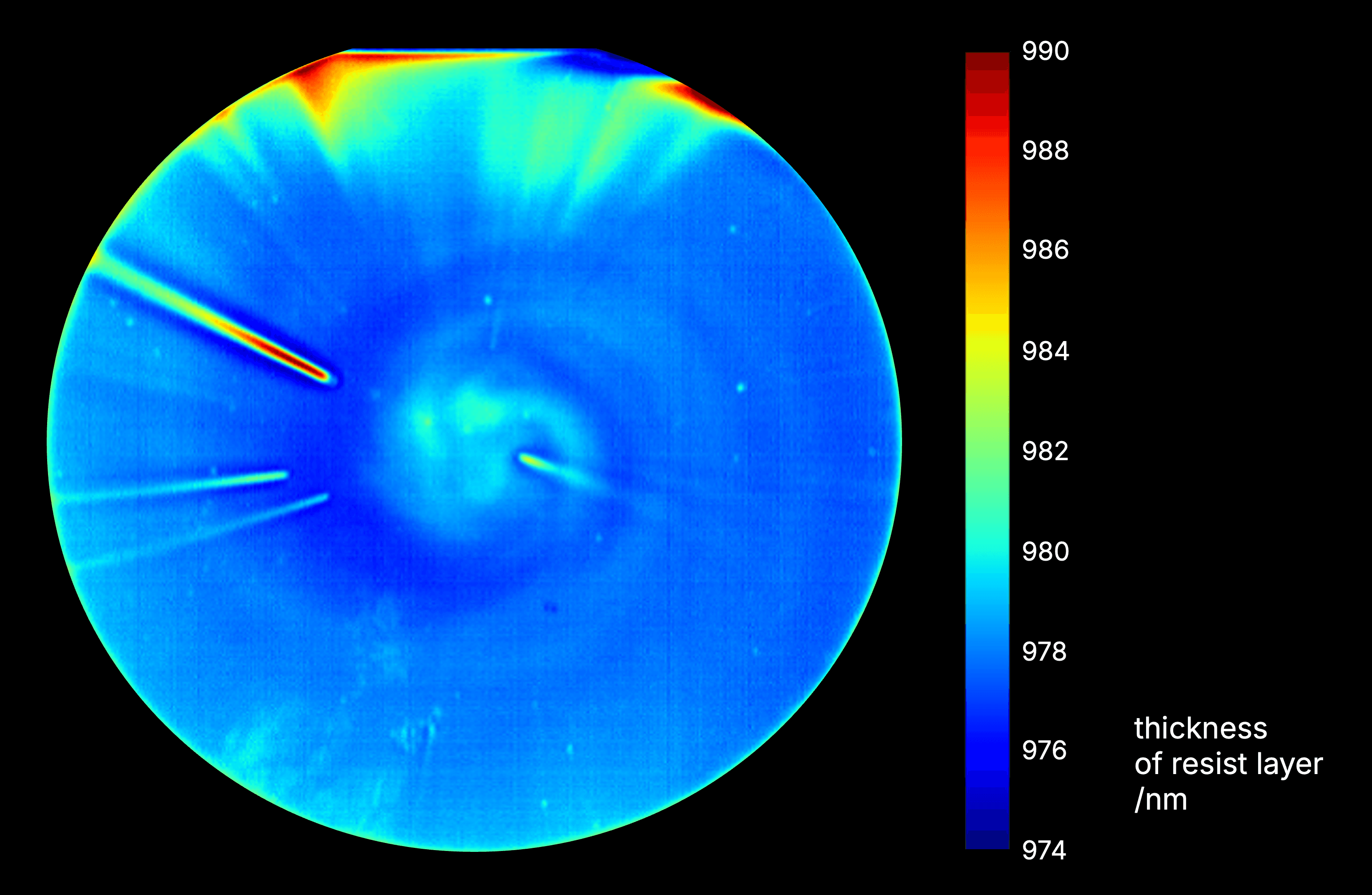
Wafer resist layer thickness uniformity was analysed using colour mapping. As depicted in the image, the resist distribution exhibits non-homogeneity, with thickness varying from 974 nm to 990 nm. The predictive model used to generate this map was trained using ellipsometry data from six sampling points across the wafer. Increasing the number of sampling points is expected to further improve the current accuracy of ±2 nm.

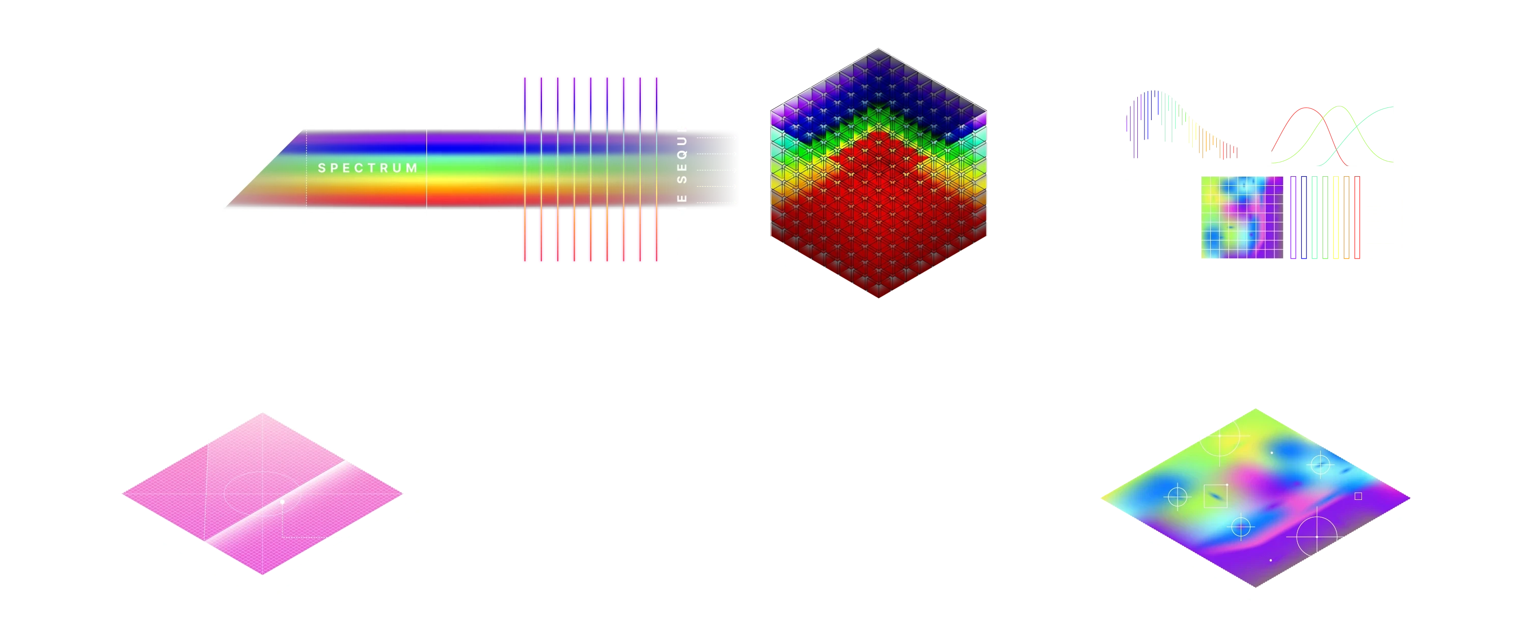
VEpioneer and VEreveal are built upon identical technological foundations and utilize our proprietary software suite, VEsolve Pro. The image below illustrates the operational workflow. Initially, data acquisition is performed via line-scan hyperspectral imaging, wherein the intensity of light reflected by the excited sample is measured. Spectral decomposition occurs within the camera, recording the intensity per pixel. Subsequent frame acquisition through sample translation results in the formation of the hyperspectral data cube. In the second phase, this data undergoes screening, exploration and analysis within VEsolve Pro, applying diverse machine learning algorithms. Finally, contingent on the selected algorithms, a wide spectrum of insights can be generated, encompassing layer thicknesses, electrical and mechanical surface properties, as well as the identification of defects and contaminants.

How the solution benefits our customers
Enhanced Reliability & Quality: Comprehensive analysis of the resist layer thickness enables continuous optimisation of the spin-coating process
Reduced Metrology Costs: Current off-line point measurement techniques which are often time- and resource intensive can be substituted
Product portfolio
VEpioneer and VEreveal systems provide spatially resolved property images of surfaces and thin films. Properties may include layer thickness, surface roughness, defects and contaminations, chemical, electrical and optical properties or any other type of quality criteria. The systems can be tailored to specific applications through customisable options for sample stage, excitation source, spectral ranges, cleanroom compatibility, and software interfaces.
Partnering with you
The DIVE imaging systems GmbH is a German manufacturer of innovative spectral imaging solutions. Our VEpioneer system is the world’s first fully integrated, one-button bench-top Hyperspectral Vision system, combining high-performance imaging with advanced data analysis to deliver insights within milliseconds. DIVE products deliver at-line and in-line inspection with highest precision and ultra-fast measuring speeds from nano- to micrometres.
We would like to thank our partners and funding bodies for their support. DIVE is funded by the Federal Ministry for Economic Affairs and Climate Protection and the European Social Fund as part of the EXIST research transfer program (funding reference: 03EUTSN217). DIVE is supported by the European Regional Development Fund and the Just Transition Fund.


